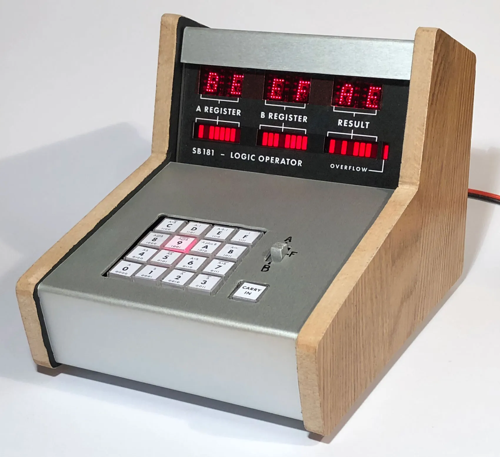
SB181: A 74LS181 based "logic operator"
I’ve had a pair of 74LS181 ALU chips waiting for a good project for a while, but the thought of building an entire CPU with them was a bit too daunting. So I’ve turned them into what I’m calling a “logic operator”: a sort of 8-bit calculator that takes hexadecimal input and displays the results to various logical functions in both hexadecimal and binary. All done with 74 series logic and no microcontroller or CPU, it makes a handy companion for the 8 bit programmer.
Circuit Explanation
A 74C923 20-key encoder chip (although it’s only connected to 16 keys) takes the user input. Depending on the position of the slide switch, the number that is entered gets stored in either the A register, B register, or the function register. The slide switch simply redirects the Data Available strobe of the 74C923 to the clock input of the appropriate register. A resistor pulls the clock inputs of each register high so that they do not trigger randomly when inactive. This Data Available strobe from the 74C923 is triggered before the actual data is present on the outputs, so I just inverted this signal through a NAND so that the registers latch on the falling edge. Otherwise the latches would always store the previously entered digit.
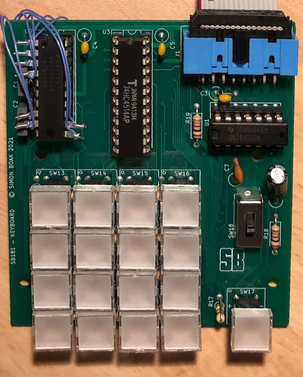
The A and B registers are both 8 bit latches each using a 74HC273. Each push of a button shifts the lower 4 bits of the register into the upper 4, and the value of the button is at the same time loaded into the lower 4. That allows for entering 2 hexadecimal digits one after the other, as you would with a calculator. The contents of these 2 registers are then fed into the A and B operand inputs of the 74LS181 ALUs. The stored values of the registers are also sent to the display board, where a pair of TIL311 display the hexadecimal value, and the binary value is shown using an LED bar graph.
The function register is a 4 bit 74HC175. While the 74LS181 ALU has many different functions, only a limited number are of any actual use. So in this case I chose the same 16 functions as agp.cooper did. An EEPROM is used as a quick and dirty way to map the 0-15 output of the keypad into the different values required by the S function inputs of the 74LS181. It also means I can choose different functions or either order on the keypad just by reprogramming it. Doing this meant I could group the functions of each button roughly together with the simpler functions at the bottom and weirder ones towards the top. The EEPROM just handles the translation.
The 4 bit output of the function register gets sent back to the keypad board. A 74HC4514 4-to-16 line decoder then connects the LED within each of the keypad switches. This illuminates it to display the currently selected function.
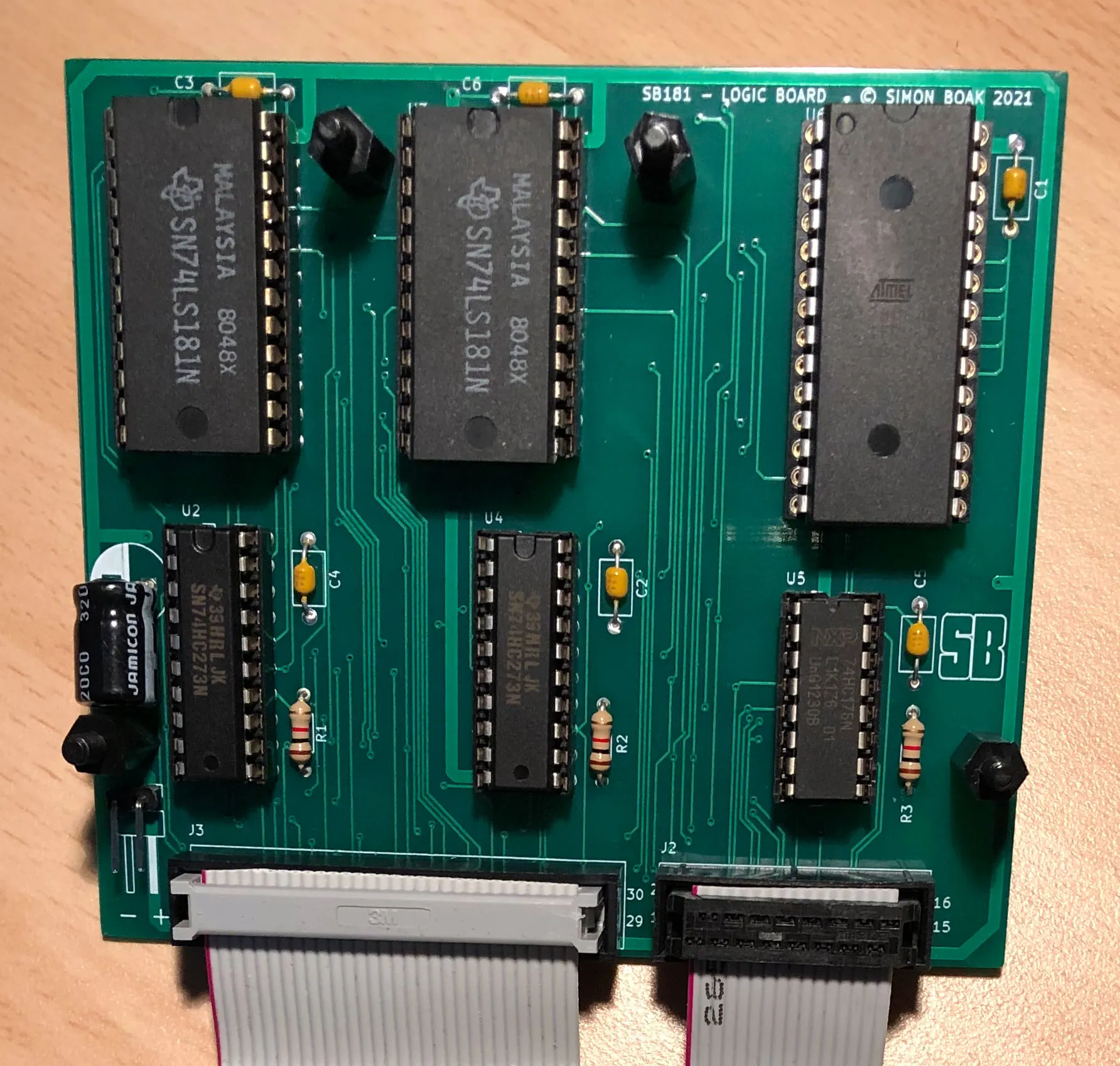
Another button is connected to a NAND gate based latch circuit. This allows for setting the carry input for the lower 74LS181. The 2 ALU chips are only 4 bits wide each, but by connecting the carry output of the lower into the input of the upper creates an 8 bit wide ALU. I don’t need to worry about any of the carry look-ahead circuitry since this is an entirely static setup with no clock or other timing to worry about.
The F output pins of the ALUs are then sent to the display board where they are shown again in both hexadecimal and binary. An additional LED shows if a carry output has been generated by the upper 74LS181.
Construction
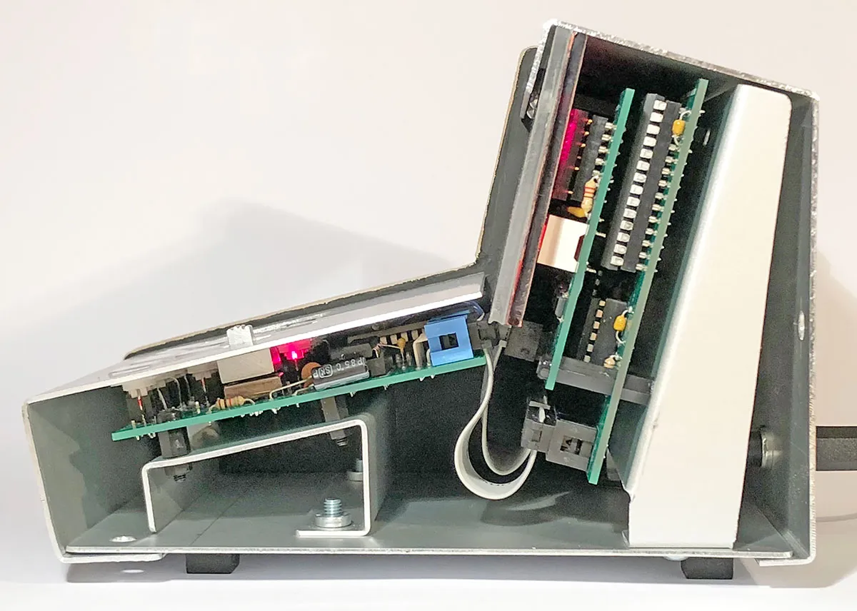
The SB181 is composed of 3 separate circuit boards. This allowed for both the relatively compact enclosure and also fitted into JLCPCB’s $2 board pricing.
The keypad board contains all of the input buttons and the register selector slide switch. I used LED illuminated switches I bought many years ago from an eBay seller in China, so I have no idea on the manufacturer or part number. The transparent key cap allows me to put a paper label behind with the hexadecimal number, the binary equivalent, and the chosen function directly onto the button. The button representing the currently selected function is always illuminated so you do not need to remember what function you have chosen.
By using the 3 position slide switch, the same 16 buttons can be used to input either operand, or select the function to apply to these operands.
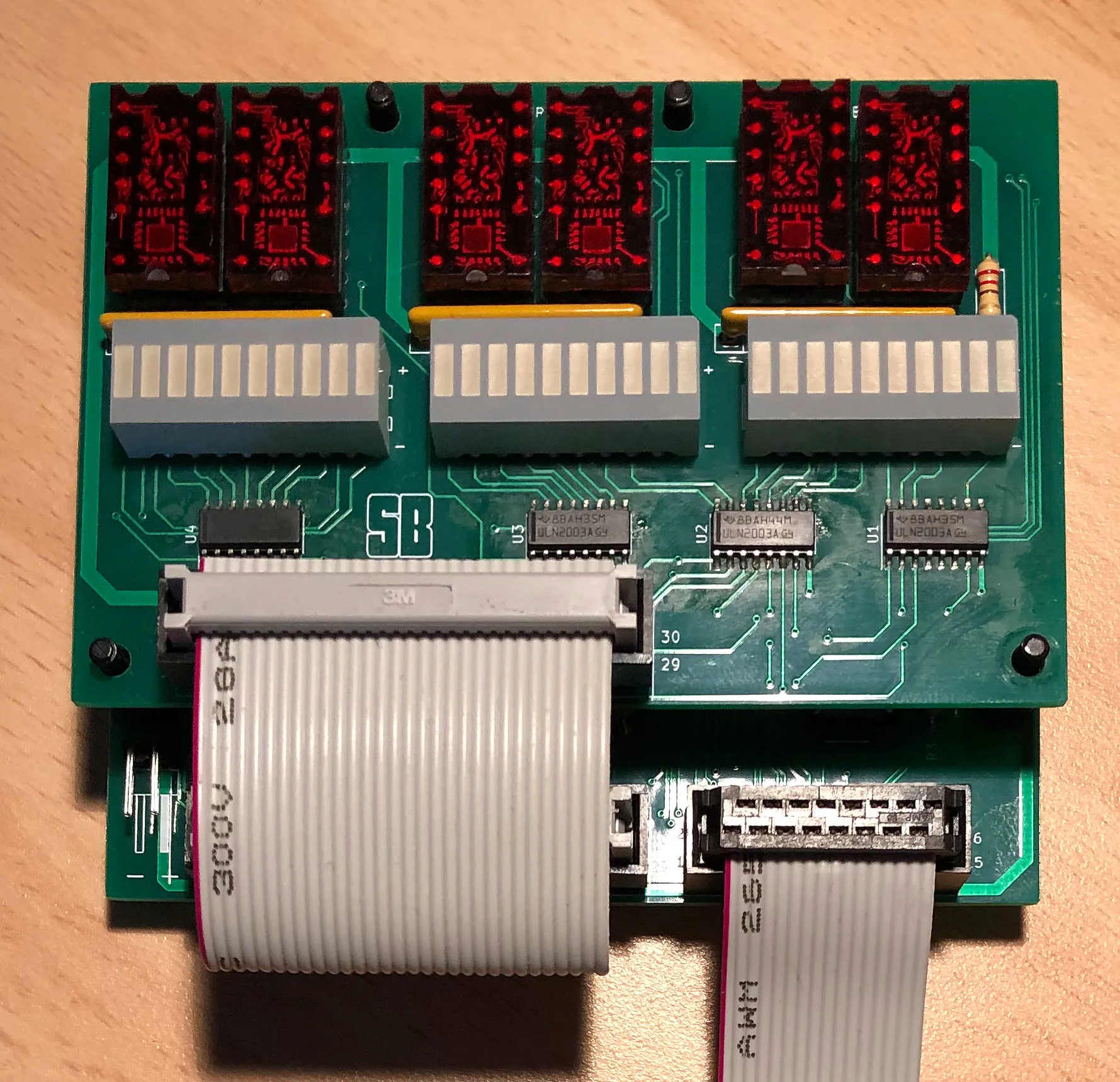
The main logic board then simply contains the 3 register latches, the function EEPROM, and the pair of 74LS181 ALUs. A ribbon cable sends the output of all of these to the display board.
The display board constantly shows the values of the 2 operands in the A and B registers, and also shows the output of the current ALU function.
TIL311 chips make for a beautiful hexadecimal display. It’s just a shame that they are so expensive to get and the amount of power they consume prevented me from being able to power this from USB. So a common eBay switching power supply circuit was used which takes a 12V input at about 750 mA and drops it to 5V. LED bar graph displays also look great for showing the binary representation, just using 8 of the 10 available LEDs, with one of the spares being used for the carry output.
I used red acrylic to give the nice consistent colour to all of the LEDs. A paper label with careful cutouts then makes it clear what the different numbers all represent. A final piece of clear acrylic on top then protects the paper.
In my schematic I mixed up and X and Y axes of the keypad encoder so I had to bodge in some wires there to ensure the numbers were in the right orientation. I also forgot that the carry output of the 74LS181 was active low, so that was also fixed by rerouting the wire on the PCB.
The main chassis is then all sheet aluminium screwed together using self-clinching nuts (my new favourite type of threaded fastener). Oak-laminated MDF then made for some suitably retro styling on the sides, which I think works well with the silvery aluminium, black labelling and red LED displays.