The world's least powerful computer? 1-bit CPU with the MC14500B industrial control unit
I came across this weird chip a few months ago. Designed by Motorola in the 70s, its purpose is to replace the “ladder logic” relays in industrial process control so all it needs to do is make simple decisions based on whether different inputs are logic high or low. It’s hard to find many references to this chip online, but I picked up some new-old stock from China (always risky) and mine are dated 2014 and made by ON Semi, which is what’s left of Motorola’s chip division.
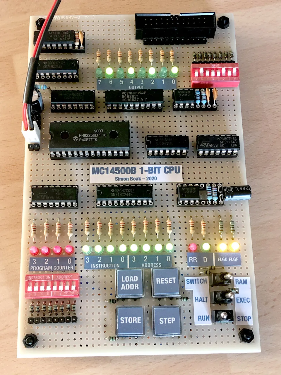
But it does contain enough of the basics to form the control logic a processor. It comes in the DIP16 form factor and is very simple to interface with. Instructions are 4 bits giving a total of 16 different instructions. A single 1-bit Result Register is the only general purpose register in the system, it comes with a WRITE flag, and a bi-directional Data register.
You must supply an external program counter so in theory there is no limit to the total address space! In my design I chose a 4 bit address space for now, so that limits my programs to a whopping 16 instructions. I only wanted this as a proof of concept, I’m not expecting to do real computing on it…
The processor instruction set allows for jumps and subroutine calls, however you must build your program counter hardware around this. I’ve ignored these for now, but it would be using the JMP and RTN pins on the chip. Currently my CPU just loops through the full program each time. The Skip Next Instruction if RR = 0 (SKZ) will still work though, so it does allow for some decision making without adding more hardware.
There are also 2 general purpose flags (0 and F) which can be used for whatever the system designer wants. In my case, I have linked these to a pair of latches connected to LEDs. The flag is only high during the single clock cycle so this means that I can use the LEDs for signalling as they will stay on after being triggered, instead of flashing and being barely visible during the clock cycle. The latches are cleared by the reset function.
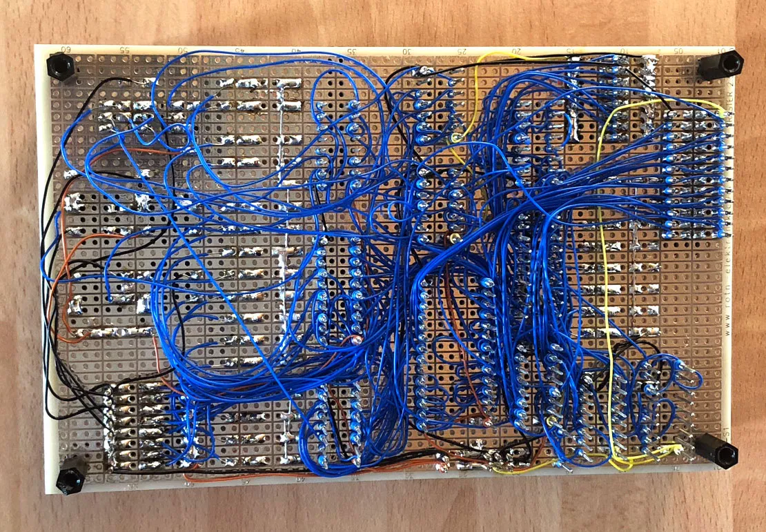
It is running at about 1 kHz. A 4-bit binary counter is the program counter and feeds addresses into the RAM chip. The DIP switches in the lower left are for loading the instruction. Leftmost 4 bits are the program instruction and the rightmost 4 bits are the I/O address. The system clock can be halted, an address loaded into the program counter, and then manually setting each 8-bit instruction word into RAM is slow and tedious. Flip the switch to “run” and watch as the LEDs blink! Program memory in RAM is completely separate from data memory, so I guess that makes this a Harvard architecture. Only 16 bytes from the 32 kB RAM chip are actually used, so it’s a bit overkill, but that’s just a RAM chip that I had going spare.
My I/O address is only 4 bits, which would limit me to only having 8 inputs and 8 outputs. However, since the devices I’m attaching to are either only read or write, I can use the WRITE line from the processor as a 5th bit. So onboard I have 8 DIP switches for inputs and 8 LEDs for output. The expansion header allows for a further 8 inputs and another 8 outputs, and also provides all the other signals I might want to attach for different types of hardware.
I don’t think the 74HC259 output latch I’m using is the right thing for the job at the moment due to its timing requirements, either that or I’ve messed up something elsewhere. But latch 0 on this chip is getting triggered at the wrong time, meaning my onboard output LED 0 is often on when a program is running. Not ideal, but works well enough for me playing around with this.
Here is a sample program which loads the value of input switches 5-7. It the saves the input value back out to the output LEDs 5-7, and also stores the complement (inverse, or opposite) of the switch value into switches 2-4. It the turns on both the 0 and F LED flags before looping back to the start and doing it all again. The first 2 instructions are also very important: this bit is only mentioned briefly in the handbook, but you won’t be able to do ANY I/O operations until you enable input and output using these instructions. Switch 0 must be on, so that the program can load this and enable I/O. This had me stuck for some time until I realised as it is not made particularly clear in the chip handbook that these are disabled on startup.
#1  IEN     $0    ; Use SW0 to enable inputs
#2  OEN     $0    ; Use SW0 to enable outputs
#3  LD      $7    ; Load the value of input SW7 into RR
#4  STO     $7    ; Save to output LED7
#5  STC     $4    ; Store the complement to output LED4
#6  LD      $6    ; Load the value of input SW6 into RR
#7  STO     $6    ; Save to output LED6
#8  STC     $3    ; Store the complement to output LED3
#9  LD      $5    ; Load the value of input SW5 into RR
#10 STO     $5    ; Save to output LED5
#11 STC     $2    ; Store the complement to output LED2
#12 NOP0          ; Do nothing for the rest of the program
#13 NOP0
#14 NOP0
#15 NOP0
#16 NOPF
So there is not much you can do with this, but it is fun to have some blinking LEDs without a microcontroller in sight. It could be possible to build a much more fully functional computer around, perhaps using it as the central controller of a wider bus, with jumps and subroutines and better I/O devices, and an ALU. I do have a couple 74LS181 chips that I’d like to use for something…